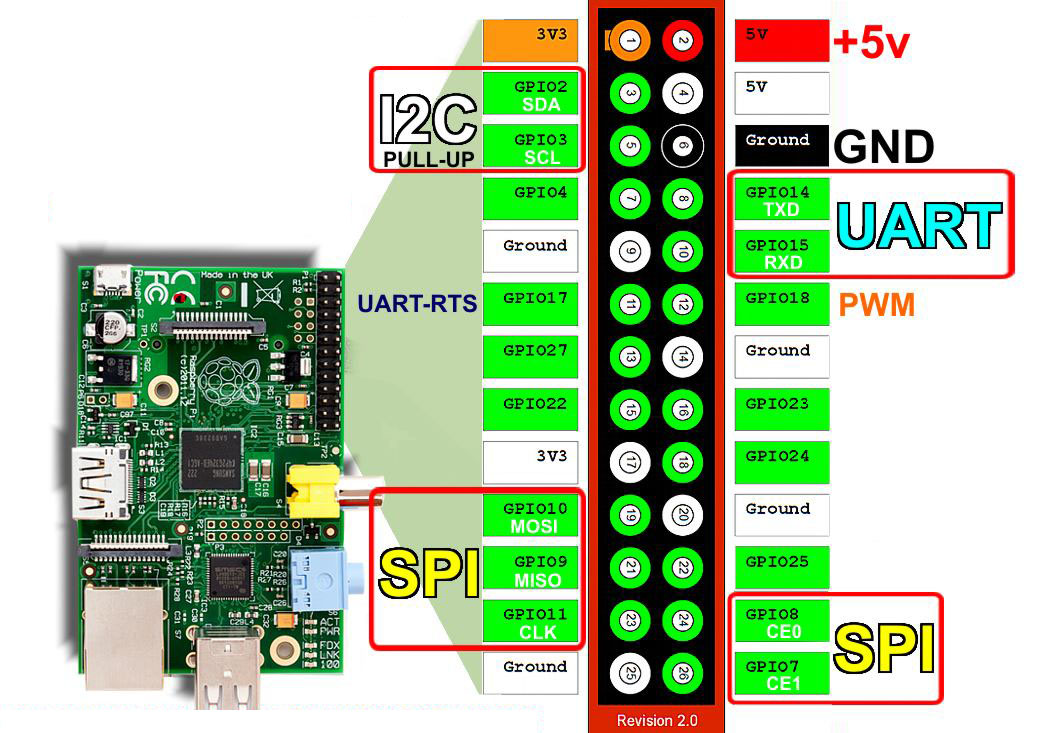
FPGAs are versatile hardware devices that allow for customizable digital logic and signal processing. One common use case for FPGAs is for controlling input and output (I/O) devices, including General Purpose Input/Output (GPIO) ports. In this answer, we will discuss how to configure an FPGA to write data from one GPIO to another GPIO.
To write data from one GPIO to another GPIO, you can use a ‘port-to-port’ connection between the input data GPIO and the output data GPIO. This can be accomplished by creating a module in your hardware design that connects the input data port to the output data port. Here is an example of how this can be done in Verilog:
    module gpio_data_transfer (
        input wire [7:0] input_data,
        output reg [7:0] output_data
    );

    assign output_data = input_data;   // Connect input port to output port

    endmodule
This example creates a simple data transfer module that passes through the data value from the input data port to the output data port through the “assign” statement.
Assuming that the design has already been synthesized and mapped, instantiate this module in your FPGA design and use the I/O pins on the FPGA to connect the input and output data ports to two separate GPIO pins. The input data value will be captured by the input GPIO and passed through the ‘port-to-port’ connection, ultimately appearing on the output GPIO.
Note that the specific implementation will vary depending on the FPGA device and development tools used. Consult the device documentation and development tools for further implementation and connectivity guidelines.
It is also important to mention that it is recommended to debounce the input gpio to eliminate any potential false transitions as the input signal is connected to a physical device. Debouncing helps improve the reliability of the signal being delivered.
In summary, to write data from one GPIO to another GPIO in an FPGA, use a ‘port-to-port’ connection between the input data GPIO and the output data GPIO. Create a module for data transfer, connect the input and output data ports to two separate GPIO pins, and instantiate the module in your FPGA design. Debouncing the input gpio is also important to eliminate any potential false transitions.
As a professional manufacturer of low power Bluetooth module, Tecksay has independently developed and produced a number of BLE Bluetooth modules that have been applied to many industries. With more than ten years of industry experience, Tecksay can customize BLE embedded solutions for customers from design, project management, function customization, system development and other aspects.


